
The printed circuit boards require a layout, whether it is in 2D or 3D. ECAD is the software that is used to create and modify the diagram and layout for assessing the PCB. The users can use this software to explore different iterations of a PCB. It can be in a sketch or a 3D layout. Users can have different options where they can compare them with.
Electrical computer-aided design is also to generate manufacturing documentations. With the introduction of the Altium designer, 18 manufacturers now can deliver user-focus, easy-to-use, and performance-enhancing PCB’s design tools.
Here are some of the new features of Altium designer 18:
High performance made simple
- For the performance optimisation design workflow is very important, and with Altium designer 18, now productivity and user experience will be enhanced with the modern interface. For the unprecedented performance optimisation, multi-threading and 64-bit architecture are all needed. If you want the design more efficient and productive than before, a modern user interface, along with updates, will work for you. It will help you in increasing routing, BOM creation, manufacturing hand-off capabilities, and rule checking. When you have the Altium designer 18, then you can have easy to use and powerful printed circuit boards design technology on your fingertips.
Properties panel
- It combines property dialogues and the inspector panel, which using selection filters to simplify access to object attributes and parameters. Object properties, snap/document option, and shortcuts are also used.
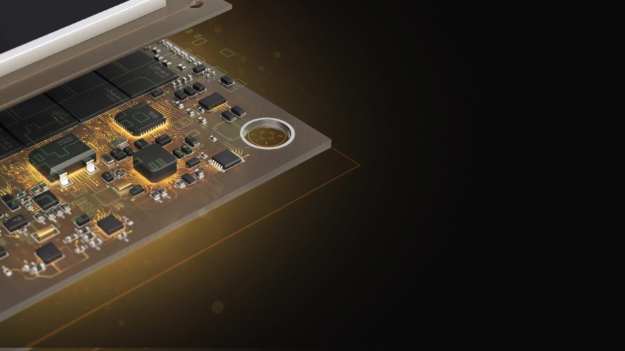
- Project A: 4-Layer, Tracks 39.6K, Components 1925, Nets 1267, Polygons 369
- Many tasks like online DRC, schematic compiler, output generation, and polygon pour now can have speed, improved task execution, and design time with the leverage of a more efficient algorithm. Now you can have the assurance of never running out of the memory.
- Active route
- ActiveBOM
- Draftsman
ECAD software provides some capabilities:
- 3D assembly capabilities help to design the 3D model of the printed circuit boards. These 3D models are used to check for interference within an enclosure. It is also used to checking for managing the dissipation of heat from electronic components on a printed circuit board.
- Trace routing capabilities are all to define the path in 2D or 3D. Switching between the layers of the printed circuit boards, the signals from the diagram embody the information between the components. It defines the location of elements in PCB.
- Diagramming capabilities helps engineers to define the purpose of using electronic components and the type of signals used to connect them.
- Collaboration capabilities deliver tools that help in a team to capture the feedback between the individual for the routing system.
- Multi-board design capability provides the design and layout for the multiple PCB’s. These numerous PCB, s work as a single system.
- Manufacturing export capabilities is for providing the ability to generate the ECAM. Which further used to make the layers of the PCB?
With the new features of the Altium designer 18 now, we can have easy and efficient PCB design tools.